Die Entwicklung aus den RCA Labors kommerzialisieren
Laut der letzten RCA Berichte aus den Bell Laboratorien arbeiteten dort rund 22.000 Mitarbeiter und es forschten tausende von Spitzen-Physikern an bislang unbekannter Technik.
Und wenn die Entwicklungen irgendwann anwendungsfertig durchkonstruiert waren, gab es die Spezifikationen in sogenannten "data sheets" für jedermann. RCA hatte betreits Patente drauf, denn die Japaner versuchten mit allen irgendwie finanzierbaren Methoden (oder Tricks) diese Patente zu umgehen oder zu unterlaufen.. Bei diesen komplexen Chips war es nicht so einfach, denn selbst die große RCA tat sich anfänglich schwer damit. Ziel waren zuerst die eigenen NTSC- Fernsehkameras.
.
Silicon Imaging Device SID 51232
General Description
RCA SID 51232 *1) is a self-scanned, charge-coupled device (CCD), solid-state image sensor intended primarily for use in generating standard interlaced 525-line television pictures.
The device contains 512 x 320 elements (163,840 individual storage sites). The device is constructed with a 3-phasef N-channel, "Vertical Frame Transfer" organization using a sealed silicon gate structure. This device features high resolution combined with ultra-low blooming characteristics.
Overall picture performance is comparable to that of 2/3-inch vidicon camera tubes but undesirable characteristics such as lag and microphonics are eliminated.
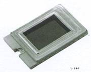
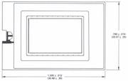
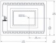
The SID-51232 is supplied in a hermetic, edge-contacted, 24-connection ceramic dual in-line package. The package contains an optical glass window which allows an image to be focused onto the sensor's 12.2mm image diagonal.
*1) Two developmental variants are available. See page 7 for grade classifications and ordering information.
.
Features
.
- 512 x 320 Element Sensor for Very Compact TV Cameras
- High Resolution
- Standard Interlaced 525-Line TV Output
- Ultra Low Blooming
- No Lag
- Precision Image Geometry
- No Microphonics
- Low Voltage and Power Requirements
- Small Size
- Highly Resistant to Image Burn-In
- Stable Sealed Silicon Gate Structure
- No Aliasing
.
Remarks :
For further information or application assistance on this device, contact your RCA Sales Representative or write Charge-Coupled Device Marketing, Lancaster, PA 17604.
Developmental-type devices or materials are intended for engineering evaluation. The type designation and data are subject to change, unless otherwise arranged. No obligations are assumed for notice of change or future manufacture of these devices or materials.
Information furnished by RCA is believed to be accurate and reliable. However, no responsibility is assumed by RCA for its use; nor for any infringements of patents or other rights of third parties which may result from its use. No license is granted by implication or otherwise under any patent or patent rights of RCA.
..
Details
.
Storage Area
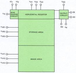
The storage area has the same construction as the image area and also contains 320 parallel vertical columns of 256 sensing cells which line up with the image area columns.
This area serves as a temporary storage site for the previous TV picture field to allow conversion of the charge pattern image into a sequential horizontal readout. The storage area must normally be covered by an external light shield.
There are three storage area clock drives. The first is ΩVB1 connected in parallel with ΩVB1'- The second and third are: ΩVB2 connected in parallel with ΩVB2' and ΩVB3 connected in parallel with ΩVB3'.
The storage area is clocked in unison with the image area during vertical blanking to transfer the complete image from the image area to the storage area (See Figure 3). During the horizontal blanking interval the entire charge pattern in the storage area is advanced toward the horizontal register by one complete cell transfer. The line adjacent to the horizontal register is loaded into the horizontal register to allow it to be read out.
.
Horizontal Register
The output register has the same 3-phase structure as the image and storage areas. The horizontal register receives one line of picture information from the storage area during each horizontal blanking interval (See Figure 3). The register contains 320 cells corresponding to each of the 320 columns in the image and storage areas plus two additional cells at the output.
Each line is clocked out at a 6.1 MHz picture element rate so that the 320 active elements are read out in the active line time of 52.7us. Typically the register is "over-clocked" by several pulses to provide a clean dark signal for video black level clamping. (Total number of pulses is approximately 335.) A bias charge is introduced into the input of the register and the signal is extracted by the output circuit.
Bias Charge Circuit
Bias charge is introduced electrically into the input of the horizontal register by the IG1, IG2, and Ois connections. When these connections are operated as shown in Figure 3, a uniform low-noise bias charge (often referred to as "Fat Zero") is introduced into the output register to maximize the horizontal resolution. This circuit provides a constant amount of charge during each clock cycle. The amount of charge is determined primarily by the difference in voltage between IG1 and IG2.
It should be noted that a bias charge is required in the image and storage areas. This is provided by illuminating the image area with a uniform background light source (i.e., a couple of LEDs placed in a position to act as a uniform diffuse light source).
.
Output Circuit
The CCD signal is extracted from the horizontal register by the circuit shown in Figure 4. OOG is the last CCD gate in the horizontal register. The CCD signal charge is collected at the floating diffusion. This diffusion is reset to a positive potential once each clock cycle by RD and 0R. The voltage change on the floating diffusion is the signal which is sensed by the output transistor. The signal may be taken from OS as a source follower or from OD as an inverter.
For measurement purposes, the photocurrent delivered by the CCD in response to a light stimulus can be measured at the drain of the reset transistor — RD.
.
Die Specs aus dem Jahr 1975
Wer immer etwas damit anfangen kann, wir haben sie hier mal eingebracht. Natürlich sind die hoffnungslos veraltet und in den 30 Jahren bis zum ersten digitalen HD Fernsehen unendlich verbessert worden, aber schaun Sie mal drüber.
.
Optical Characteristics
| Image Cell Size | 1.2 x 1.2 mils (0.03 x 0.03 mm) |
| Image Size (3x4 aspect ratio) | 288 x 384 mils (7.31 x 9.75 mm) |
| Image Diagonal | 12.2 mm |
| Effective Optical Distance from Socket Top (See Figure 9) | approx. 100 mils (2.54 mm) |
| Minimum Useful Wavelength | 420 nm |
| Maximum Useful Wavelength | 1100 nm |
| Saturation Exposure | 2.67 x 10 hoch -3 fcs 2856 K |
.
Typical Performance Data
Conditions: Standard EIA RS-170 525-line TV format operating at 25°C.
| Electrical Parameter | Unit | Note |
| Horizontal Clock Rate | 6.1 MHz | |
| Video Bandwidth | 3.0 MHz | |
| Vertical Transfer Rate | 0.28 MHz | |
| Light Integration Time | 16.67 ms | |
| Image Area Dark Current | 4 nA | 1 |
| Image Area Light Bias Current | 30 nA | 1 |
| Peak-to-Peak Signal Current | 250 nA | 1 |
| Peak-to-Peak Signal Voltage | 12.5 mV | 2 |
| Saturation Peak-to-Peak Signal current | 400 nA | 1 |
| Horizontal Register Bias Current | 300 nA | 1 |
| Horizontal Limiting Resolution | 240 TVL/PH | 3 |
| Vertical Limiting Resolution | 480 TVL/PH | 3 |
| Contrast Transfer Function (CTF) | 0.4 - | 4 |
| Gamma | 1 - | 5 |
| Signal-to-Noise Ratio | 50 dB | 6 |
| Optical Sensitivity (Luminous) | 3250 jUA/lm | 1,7 |
| Sensitivity (Radiant) 65 mA/W-2856 K | 1,7 | |
| Faceplate Illumination (250 nA signal) | 0.1 fc | 7 |


