
Ein ganz früher sehr detaillierter Artikel vom April 1974
Das "Silicon Image Device" ist etwa 1970 in den Bell Laboratories in USA entdeckt - erfunden und/oder entwickelt worden. Ursprünglich sollte es eine neue Art von Halbleiter- Daten- Speicher werden, um Computer Daten besser (schneller) als bisher abzuspeichern und dann noch schneller wieder abzurufen. Wie dann der Weg zum optischen Sensor verlief, ist an anderen Stellen aber nur rudimentär beschrieben. Hier haben wir einen Artikel von "R. L. Rodgers, dem III" gefunden.
- Manuscript received April 24, 1974. This paper was presented at the 1974 IEEE Intercon in New York (March 1974).
Über R.L.Rodgers, "den Dritten" at RCA Laboratories


R.L. Rodgers III, Manager, CCD Manufacturing and Engineering, Electro-Optic Products, Lancaster, Pa., received his training in physics and electrical engineering at the Polytechnic Institute of Brooklyn. He has been working on electrooptic imaging devices since joining RCA at RCA Laboratories in 1964. He was instrumental in the conception and design of RCA's Silicon Vidicon and "Silicon Intensifier Target" (SIT) camera tubes.
He transferred to the Electro-Optic Products Advanced Technology area in Lancaster in 1969 to continue work on silicon camera tubes and LLL-TV cameras using these tubes, resulting in the development of a photoelectron noise limited I-SIT camera.
He was responsible for the development of an effective non-bloominq silicon target design and new lower cost fabrication techniques for silicon targets. Most recently he has been involved with "Charge Coupled Devices" (CCDs) for imaging and memory applications. He was promoted to his present position early in 1974. Mr. Rodgers has presented many technical papers and received an RCA Laboratories Achievement Award in 1968.
.
Charge-Coupled Imager for 525-Line Television

by R.L.Rodgers - The operation and performance parameters are described for a CCD image sensor having 512 x 320 elements (163,840 individual storage sites).(Bei uns sind das heutzutage die "Pixel".) The device is designed and fabricated for use in the standard 525-line television system.
This solid-state imager is capable of performance superior to that of camera tubes with regard to signal-to-noise ratio, freedom from lag, and absence of microphonics. Additional features include its small size, light weight, low power, and precision image characteristics.
.
Der Chip wurde ganz gezielt fürs NTSC Fernsehen entwickelt
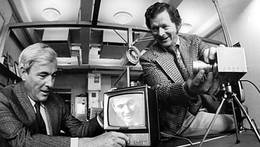
- Ein Foto aus 1974 - die beiden US-Forscher Willard Boyle (links) und George Smith (rechts) bei einem Versuchsaufbau mit einem CCD-Sensor

Considerable effort went into the development of a tv system that would make an acceptable picture utilizes all of the eye-brain visual perception principles. Factors such as the visual acuity of the eye and critical flicker frequency effects were considered.
This effort led to the development of the U.S. Standard 525-line television system. For a "solid-state image sensor" to obtain its greatest market potential it should be compatible with and meet the minimum performance parameters of this standard system.
Many approaches have been taken toward achieving this goal. The most promising approach thus far is a charge-coupled imager which has the potential for meeting both performance and manufacturing requirements.
The production experience with silicon vidicon targets will provide a base for the manufacture of solid-state charge-coupled image sensors. *1).
.
Die ersten Spezifikationen aus der NTSC Welt
The 512 X 320 element CCD imager containing 163,840 individual analog storage sites has been designed and fabricated for the requirements of the standard 525-line television system. In this paper, the requirements for this system are defined and the resultant imager performance is described.
Several smaller size vertical frame transfer CCD imagers were developed prior to the 512 X 320 imager *2), *3), *4). These devices demonstrated that the required device performance parameters could be obtained.

.
Dies ist eine Tabelle aus Deutschland. Hier werden die nominellen Zeilen-Normen spezifiziert. Von diesen "nominellen" 525 oder 625 Zeilen werden sowieso nicht alle übertragen, sondern nur die sichtbaren Zeilen. Und dann ist das immer noch kein Maß für die effektive Resolution, die Auflösung in "Linien", die am Ende wirklich sichtbar und unterscheidbar im professionellen Studio-Monitor bzw. im Heim-Fernseher zu sehen sind.
.
Image sensor requirements for 525-line tv compatibility
The television system used for almost all broadcast and closed circuit television in the United States is the system described by the National Television System Committee (NTSC). This standard is described in EIA standards RS-170 for broadcast and RS-330 for closed circuit industrial applications. For the purpose of the following discussion, the requirements are the same.
The standard RS-170 system consists of two 262.5 line fields each 1/60 second long (1/59.939 second for color), interlaced 2:1 to form one complete frame every 1/30 second. Approximately 23% of each frame is devoted to blanking time for the display. This time is used to transfer charge from one register to another in a CCD.
Vertical cell count
The RS-170 vertical blanking interval is .075 ± .005 of the field interval yielding 241.5 to 244.125 (243 nominal) active display lines per field.
Hier wird zur weiteren verwirrung von "active display lines" gesprochen.
This places a requirement of a minimum of 242 lines to be generated by the imager for each field. The maximum number of lines in each field is 262 to enable all of the cells for that field to be read out before the next field starts.
One row of cells is required for each line in the display. The RS-170 sync pulses cause the display to interlace each field with the preceding field. This causes a display with approximately 486 active lines per frame. The same 243 line positions generated on one field may be repeated on the next field giving a 486 active line display, with the resolution of 243 lines, or a new interlaced set of 243 elements may be supplied by the sensor (each field) for a total of 486 lines of vertical resolution per frame.
.
Die Übersetuung ist gar nicht mehr trivial, weil hier von Feldern anstelle von zum Beispiel Frames oder Einzelbildern gesprochen wird.
.
Horizontal cell count
The RS-170 standards call for a horizontal line frequency of 15,750 lines/s (15,734 lines/s for color). The line time is therefore 63.49 microseconds. The nominal horizontal blanking interval is 17% of the horizontal line time leaving 52.7 microseconds active display time.
In closed circuit applications, the horizontal video bandwidth is unlimited. In monochrome and color broadcast, the luminance bandwidth is 4.2 MHz. Filling this bandwidth requires approximately 450 cells.
A composite color signal has the color information modulated on a 3.58 MHz subcarrier. Unless the video monitor or receiver uses an expensive comb filter to remove the chroma information from the luminance signal (not commercially used), the color subcarrier beats with the luminance signal causing an annoying edge creep.
It is therefore common practice to limit the luminance video bandwidth to 3 MHz. Most present-day video tape recorders are also limited to 3 MHz video bandwidths for luminance information.
This leads to a practical minimum number of cells for the 3 MHz bandwidth of 320 cells. The corresponding video data rate is 6 MHz. Table I summarizes the 525-line system requirements.
.
Picture format considerations
There are several factors affecting the choice of picture format.
Table II lists the most popular formats used in television, movie film, and still photography. Most movie film and tv formats have the 4:3 aspect ratio which is required for the standard tv system.
There has been a general trend towards smaller formats through the years in all three media. This has been the result of improvements in the resolution of lenses and photosurfaces as well as the need "for more compact and lightweight equipment.
.
Most popular lenses are the "C-mount" variety
The most popular lenses are the "C-mount" variety. There are two basic subdivisions of C-mount lenses.
These are the designs for the 16mm format of one inch vidicons and 16mm movie film. Any of the 16mm vidicon lenses can however be used for the smaller formats.
The 11-12mm formats seem very attractive because of their small size and ready availability of inexpensive interchangeable lenses. Lenses for 8mm and Super 8mm have low MTF's in the tv line ranges of interest and the small format requires extremely small CCD cell dimensions — beyond the state of the art for fabrication and device operation considerations to achieve standard tv resolution (240 television lines per picture height).
Hier ist die weitere - aber zur Unterscheidung wichtige - Benennung der "lines" erwähnt, bei uns sind das die so benannten "Linien" im Vergleich mit den "Zeilen".
An additional drawback of very small formats is the inability to achieve selective focus special effects with normal fields of view due to the inherent very large depth of focus.
.
Tabelle 1 - Die NTSC Spezifikationen aus US Sicht
Table I — Summary of 525-line television system requirements (RS-170).
.
Vertical Parameters
.
- Frame Time (1/30 Second)
- 2 Interlaced Fields (1/60 Second Each)
- Total Number of Lines Per Field (262.5)
- Vertical Blanking Interval (.075 ± .005 V)
- Active Scan Lines Per Field (Nominal/243)
.
Required Vertical Cell Count:
.
- 242-262 Each Field (Repeated or Interlaced)
.
Horizontal Parameters
.
- Luminance Electrical Bandwidth (4.2 MHz)
- Color Receiver and VTR Practice (3 MHz Bandwidth)
- Required Cell Count:
- 4.2 MHz (Approx. 450 Cells) 3 MHz (Approx. 320 Cells)
.
Format Parameters
.
- Picture Aspect Ratio (4:3)
.
512 x 320 CCD imager performance parameters
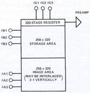
- Fig. 1 - Layout of 512x320 element CCD imager.

A 512 x 320 element CCD array has been designed and fabricated for the standard 525-line tv system as described above. It is capable of generating the full resolution requirements of broadcast color receivers and tape recorders.
Hier wird darauf hingewiesen, daß mit dieser Pixel-Zahl die erforderlche volle "Auflösung" des NTSC Fernsehbildes erreicht wird. Fig. 1 shows the layout of this vertical frame transfer imager.
The imager is composed of three sections. The lower section contains 256 x 320 cells which can be interlaced on alternate fields to generate 512 x 320 picture elements per frame *5).
In actual use, only 486 lines (243 per field) are displayed as described above. The extra elements are provided to allow variations in system blanking and timing and to avoid non-uniformities at the picture edges.
The middle section contains a 256 x 320 cell storage area to provide format conversion to a sequential horizontal readout. The top section shows the 320-element readout register, which shifts the video out at 6 MHz data rate.
The cell size is 1.2 x 1.2 mils resulting in a 12mm image format. The overall chip size is 500 mils x 750 mils.
.
Tabelle 2 - Die bislang bekannten Bildformate
Table II — Popular image formats
.
| Movie Film | Format (Diag.) | Aspect Ratio |
| 8 mm | 5.46 mm | 4:3 |
| Super 8 mm | 6.68 mm | 4:3 |
| 16 mm | 12.0 mm | 4:3 |
| 35 mm | 25.5 mm | 4:3 |
| Television | ||
| 2/3" Vidicon | 11.0 mm | 4:3 |
| 1" Vidicon | 15.9 mm | 4:3 |
| 1.2" Vidicon | 21.2 mm | 4:3 |
| 1.5" Vidicon | 25.0 mm | 4:3 |
| Still Film | ||
| 110 | 21.2 mm | 4:3 |
| 126 | 39.2 mm | 1:1 |
| 135 | 43.3 mm | 3:2 |
.
Spectral response
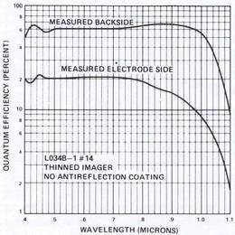
- Fig. 2 - Spectral response of CCD imager; wavelength is in micrometers.

The spectral response of a CCD is similar to the spectral response of a silicon vidicon. The spectral response extends from a 0.4 µm to 1.1 µm. Fig. 2 shows thr spectral response for a thinned area imager test device.
Absorption of light in the transfer electrodes reduces the available light to the substrate when an image is formed on the electrode side. When the light is incident on the backside (side opposite transfer electrodes), the deviation in sensivity from 100% quantum efficiency is caused primarily by reflection losses and incomplete absorption in the infrared.
The magnitude of light loss in electrode side imaging varies with process variations and wavelengths, and can differ somewhat from that shown in Fig. 2, particularly in the blue end of the spectrum. The backside illumination is basically independent of electrode details.
.
The SIT-CCD
A vertical frame-transfer CCD imager processed for backside illumination that has good blue response may be fabricated into a new type of high-sensitivity CCD imager. This device is the CCD version of the Silicon Intensifier Target (SIT) Camera Tube *6).
The SIT-CCD imager consists of a photoemissive cathode, electron-optical focusing section, and CCD imager in an evacuated envelope. The photoelectron image is injected into the silicon at high energy, forming many secondary hole-electron pairs. This current gain greatly increases the sensitivity of a CCD by raising the output signal above background signal variation limitations. Interline-transfer CCD imagers cannot use this method of low-light-level sensitivity enhancement.
.
Resolution
The most basic limitation on limiting resolution is the number of cells contained in the imager. (Heute sprechen wir von der Zahl der Pixel.) In the horizontal direction, the number of cells is determined by the number of channels formed by the channel stop diffusions (320 for the 512 x 320 device).
In the vertical, the number of resolution elements is determined by the number of different storage cell configurations formed by the transfer electrodes in the image area (256 actual cells electronically interlaced 2:1 to achieve 512 sample positions in the vertical direction).
Resolution is usually defined in terms of Television Lines / Picture Height (tvl / ph). In the horizontal direction, this number is 3/4 of the horizontal cell count or 240 tvl/ph due to the 4:3 aspect ratio.
In the vertical direction, only 486 resolution samples are displayed out of the 512 possible, and the finite line structure in the display is often quoted as reducing the effective useful resolution to approximately 350 tvl/ph due to the kell factor even though actual resolution may be seen to the 486 sample limit with proper pattern phasing. In the horizontal, the video is smoothed into a continuous waveform and the finite cell (moire) effects are not as severe.
Ein weiterer Faktor bezüglich der Auflösung ....
Another factor affecting picture sharpness is the reduction of MTF (sine wave response) due to resolution loss mechanisms in the image formation and readout processes.
These losses are tabulated in Table III for a 1.2 mil cell dimension. The lens is the first contributor to the loss of resolution in image generation.
The lateral diffusion of electrons in the imager before collection is the second mechanism. It is a "Sech"-function of the optical spatial frequency and field-free diffusion length in the bulk. The numbers shown are representative of typical geometries.
The third loss is the Sin X/X loss due to the finite cell sampling process. All of these effects are also present in silicon vidicons *1).
The resolution losses in the readout process are given by the equation in Table III. "Ne" is the transfer loss and "fe" is the frequency of one cell. This resolution loss mechanism is analogous to the resolution loss of a scanning electron beam in a silicon vidicon.
The overall MTF is the product of the image formation MTF and the readout MTF. The squarewave response CI F is larger than the sine-wave response MTF. The actual measured responses depend on the phasing of the light pattern with respect to the cell pattern. If the black-and-white bars are lined up with the cells in an in-phase condition, the response is greatest.
If the bars are lined up with half a white bar and half a black bar contained in each cell, the response at the cell limit will be zero.
.
Transient response
In the vertical frame transfer design, the picture is integrated for one field (16.66 milliseconds). The picture is then read out completely each field. There are therefore no smearing effects due to lag during panning except for resolution loss due to image motion during exposure as in any movie film camera.
Some other types of solid-state sensors integrate for a full frame (33.3 milliseconds) and have twice the panning resolution loss because of the longer exposure time.
.
Dark current
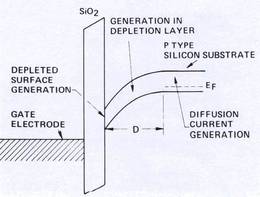
- Fig. 3 - Dark current sources in CCD imagers.

During the operation of a CCD imager, a two-dimensional charge pattern replica of the light pattern is formed inside the CCD. Thermally generated charge partially fills the potential wells and generates a background signal known as dark current.
There are three basic dark-current generating mechanisms. These sources are illustrated in Fig. 3. The first source is diffusion current from the substrate. This current source can be neglected. The second source of dark current is from the depleted layer between the "SiO2" interface and the substrate.
A simplified equation for this current density is ??? = ?????, where r is the effective lifetime and Nt is the intrinsic carrier concentration. The effective lifetime is a complex function of the actual hole and electron lifetimes and the energy level of the generation centers.
If CCD's are processed to remove most of the generation centers near the center of the bandgap, this component of dark current is less than the third dark-current source.
The third dark-current source is generation current from surface states at the silicon SiO2 interface. A simplified equation for the surface-generation current density is ??? = ???. S is the effective surface generation velocity and is proportional to the surface-state density NSs near the middle of the bandgap. The value of Nss near the center of the band may differ significantly from the density of surface states nearer the band edges which affect transfer efficiency. Actual dark current measurements have yielded dark current densities of 5 nA/cm2. This results in a dark current of about 4 nA in the image sensing area of a 512 x 320 cell device.
The second and third dark-current sources depend on the temperature variation of Ni. This results in the standard silicon dark-current variation of a factor of 2 for every 10°C temperature change around room temperature.
.
Blooming
CCD's exhibit unique problems of charge containment when overloaded with light. Charge is fairly well confined from spreading sideways by the channel stop diffusions. However, excess charge can spill up and down the channel.
A special mode of operation has been developed to greatly reduce the spreading of charge down the channel under overload conditions. This low-blooming mode is accomplished by maaintaining the phase fingers adjacent to a charge integrating phase finger at a voltage that maintains the surface under these fingers in light accumulation. This forms a temporary extension of the channel stop around each charge intergration collecting site minimizing charge spread down the channel.
.
On-chip video processing
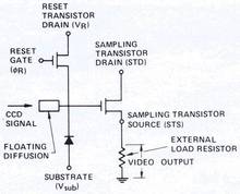
- Fig. 4 - On-chip video processing.

The charge signal in a CCD is manipulated around without touching a finite electrode until it is extracted at the output. A floating diffusion is used as a charge detector. The voltage on the floating diffusion is reset to a fixed potential once each clock period by a reset transistor.
When each charge packet reaches the floating diffusion, the charge changes the voltage on the capacity at that node. This voltage is sampled by a sampling transistor operating as a source follower. These circuits are shown in Fig. 4. The very low node capacity of the floating diffusion results in a significant improvement in signal-to-noise ratio over a silicon vidicon operating at the same light level. In fact, at normal signal levels, no noise is visible in a displayed picture generated by the CCD imager.
.
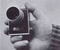
Developmental camera
A developmental black-and-white camera has been fabricated for the 512 x 320 CCD imager. Fig. 5 shows a picture of this camera. The camera is approximately the size of a pack of cigarettes and has a C-mount for lens interchangeability. Fig. 6 and Fig. 7 show 525-line monitor pictures made by this camera with a 512 x 320 CCD imager.
.
- Fig. 5 - View of the black-and-white camera for the 512x320 CCD imager.

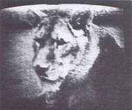
- Fig. 6 - A 525-line picture made with the 512x320 CCD imager.

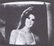
- Fig. 7 - A 525-line picture made by the 512x320 CCD imager.

Summary and conclusions
A CCD imager has been developed that will offer an attractive alternative to camera tubes for many 525-line television applications.
It is capable of supplying the full resolution of color tv (240 tvl/ph). The features of CCD imagers that are superior to camera tubes are signal-to-noise ratio, freedom from lag, and absence of microphonics (soetwas kommt nur in Aufnahmeröhren vor) . The small light weight, low-power consumption, and precision image characteristics are additional benefits. Table IV summarizes the performance parameters for this developmental 512 x 320 CCD imager.
.
- Anmerkung : Hier nochmal der Hinweis, daß die Bezeichnung "240 tvl/ph" - also der Zusatz "TV-Lines" !! bei uns die Anzahl der Linien sind, die die echte Auflösung spezifizieren.
.
References
.
- 1. Rodgers, III. R.L., "Beam Scanned Silicon Targets for Camera Tubes," Paper presented at IEEE Intercon, New York. NY, March I973.
- 2. Weimer, P.K., Pike, W.S., Kovac, M.G., AND Shallcross, F. V., "The Design and Operation of Charge-Coupled Image Sensors," Paper presented at IEEE Solid State Circuit Conference, Philadelphia, Pa., February 1973.
- 3. Kovac, M.F., Shallcross, F.V., Pike, W.S., and Weimer, P. K.., "Design, Fabrication, and Performance of a 128X 160 Element Charge Coupled Image Sensor," Paper presented at CCD Applications Conference, San Diego, California, September 1973.
- 4. Tompsett, M.F., Amelio, G.F., Bertram, W.S., Buckley, R.R., McNamara, W.J., Mikkelsen, Jr., J.C., and Sealer, D.A., "Charge-Coupled Imaging Devices: Experimental Results," IEEE Trans. Electron Devices, Vol. EIV^ pp.992-996, November 1971.
- 5. Sequin, C.H., "Interlacing in Charge-Coupled Imaging Devices, " IEEE Trans. Electron Devices, Vol. ED-20, pp. 535-541, June 1973.
- 6. Rodgers, 3rd, R.L., et ah "Silicon Intensifier Target Camera Tube." Paper presented at IEEE International Solid State Circuits Conference, Philadelphia, Pa.
.