

RCA - "BROADCAST NEWS" -
Vol. No. 76 September 1953
published by RADIO CORPORATION OF AMERICA - BROADCAST & TELEVISION EQUIPMENT DIVISION, CAMDEN, NEW JERSEY. - Copyright 1953
Bei uns ist dies eine der ersten Ausgaben der "RCA News".
Diese RCA "Broadcast News" beschäftigten sich über 30 Jahre nur mit sogenannten AM-Sendern und den zugehörigen US-Rundfunkstudios, die von RCA eingerichtet worden waren. Nach dem Durchbruch des Mittelwellen-Rundfunks Mitte der 1930er Jahre war die RCA eine der treibenden Initiatoren und auch eine der Hauptprofiteure von diesem Aufschwung.
Natürlich war das vor allem dem Tatendrang und Geschick des RCA Chefs David Sarnoff zuzuschreiben, der alle Hebel in Bewegung gesetzt hatte, daß an RCA (in den USA jedenfalls) niemand mehr vorbei kam. Mitte der 1940er Jahre gab es in den 49 Staaten der USA über 3.500 Radiostationen, von lokalen Kleinstsendern mit 10 Watt Sendeleistung bis zu ganzen Netzwerken von Stationen mit 50 KW und mehr wie NBC, ABC, CNN usw..
Und RCA belieferte jeden, der es bezahlen konnte. Die US-Dollar- Preise solcher Sender kommen auch noch. Weiterhin ist wichtig zu wissen, die großen amerikanischen Hochtechnologie- Labors waren alle in der New Yorker Gegend angesiedelt, die von Bell und von RCA und auch einigen Universitäten wie Princeton (Albert Einstein lehrte dort).
Und in den Bell Labs von AT&T und Western Electric wurde um 1947/48 der Transistor erfunden oder entdeckt. Und die RCA-Labors waren ja quasi nur um die Ecke.
.

.
Sept. 1953 - SURVEY OF TRANSISTOR DEVELOPMENT
(Ein Überblick über die Entwicklung des Transistors)
By B. N. SLADE - staff member of the David Sarnoff Research Center of RCA at Princeton, N. J. - Tube Division Radio Corporation of America Harrison, N. J.
.
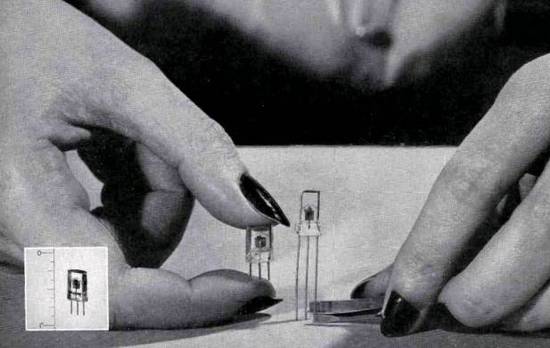
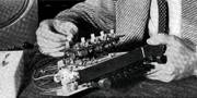
- FIG. 1. Less than half the size of a metal paper clip, the diminutive transistor points the way to development of many types of miniaturized electronic equipment.

Editor's Note :
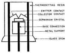
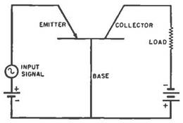
- FIG. 2. Construction details of the RCA developmental point-contact transistor.

From time to time we have had requests from readers for an anthoratativc article on transistors. After looking into the subject we decided that the best introductory article on this subject was one written a little over a year ago by B. N. Slade of our Tube Division and which appeared in RADIO AND TELEVISION NEWS originally.
In reproducing this article here we have added a number of illustrations not originally included. Most of these are photographs of transistorized equipment items produced by RCA Laboratories. They are included to give an idea of the kind of products in which transistors may be used commercially at some time in the future.
It should be noted that since this article was tvritten further progress in transistor development has occurred. It is our intention to cover these more recent developments in a second article which will appear in a forthcoming issue.
* Reprinted in part from "Radio and Television News," September, October and November, 1952 issues.
.
- Anmerkung : Schon in diesem frühen Artikel ist der Kern-Context so formuliert, als wenn RCA diesen (oder "den") Transistor erfunden hätte. Diese Denk- und Schreibweise wird uns noch öfter in den RCA "Broadcast News" auffallen.
.
- 2. Anmerkung : Weiterhin hatte der Autor Mr. Slade (oder sein Nachfolger) große Probleme mit der Reihenfolge und der Zuordnung der Bilder und Grafiken zum jeweiiigen Thema im Text. Er hatte die ursprünglich alle kreuz und quer in den langen Text rein geklatscht. Das ist hier zwar korrigiert aber dennoch etwas verwirrend.
.
Kein Wort von den 3 Erfindern in den BELL- und AT&T- Labors
- FIG. 4, Side view of the experimental portable battery-operated television receiver. Housed in a cabinet 12 x 13 x 7 inches about the size of a portable typewriter case - its weight is 27 pounds. It operates from a self-contained loop antenna.


- FIG. 5. The portability of an experimental battery-operated television receiver which uses transistors and no tubes - except the kinescope - is demonstrated by George C. Szeklal.

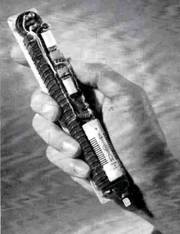
- FIG. 6. In the foreground, a unit of an experimental "Walkie-Lookie" in comparison with a corresponding tube-equipped unit which was used in earlier experiments. Seventeen point-contact transistors perform the function of twenty-two tubes.

- FIG. 7. A cigar-size experimental microphone-transmitter, modulated by a tiny built-in dynamic microphone. Employs two developmental junction type transistors, coil and battery.

As a result of the progress made in the design and manufacture of the transistor, a germanium-crystal triode, this electronic device looms (sich abzeichnen) today as a desirable supplement to the electron tube in many applications.
The development of the transistor may make possible new types of electronic equipment which will use not only transistors, but also electron tubes, and other electronic components in increasing quantities.
In fact, the commercial application of transistors appears to be not too distant, although a considerable amount of time is probably still required before these units become commercially available on any sizable scale.
.
The advantages of transistors
The intense interest in the transistor shown by electron-tube research and development engineers may be attributed to the fact that the transistor performs functions similar to those of triode-type electron tubes, although the mechanism of conduction is quite different.
The transistor is of particular interest to equipment designers, who see many circuit possibilities in its characteristics. It is very small in size, and the power requirements for its operation are extremely low. When suitable circuits are developed, space and power requirements for complex electronic equipment may be simplified to a large degree by the use of transistors.
Another promising feature is that the operating life of certain types of transistors shows indications of being very long (compared by tubes), thus minimizing replacement problems. The physical ruggedness of the transistor offers other obvious advantages. In addition, the transistor requires no "warm up" time but will operate instantaneously upon application of voltage to its electrodes.
.
A view onto the disadvantages of germanium
The limitations of the present developmental transistors, however, must not be overlooked. Transistor characteristics vary with ambient temperature changes, the noise is high compared with that of electron tubes, and the power output is relatively low.
Nevertheless, when the favorable characteristics of the transistor are weighed against its limitations, it appears that this device, even in its present developmental stage is destined for use in many applications. Further improvements in its characteristics undoubtedly will create new and expanding fields for its use.
At the same time, the principles of semi-conduction in solids may be expected to play an increasing part in the development of many new electronic devices, of which the present transistor is but the first.
.
Two types of transistors .......
Two types of transistors,
.
- the point-contact type and
- the junction type,
.
will be discussed in this series. The point-contact transistor will be discussed first, and at greater length, because the development of this device has reached a more advanced stage and more is known about its performance with respect to frequency of operation, life, and uniformity of characteristics.
However, the junction transistor promises to be at least as important as the point-contact transistor in many applications.
.
The germanium crystal
The heart of the transistor is the germanium crystal. Germanium is a semi-conductor, a metallic-like substance having conductivity greater than that of an insulator but less than that of a conductor. Its resistance, in contrast with that of metals, decreases as its temperature is raised. Other types of semi-conductors, such as silicon, lead sulphide, and selenium, have been used in transistor work, but, to the present time, germanium has proved the most successful.
Germanium is known mostly for its use in point-contact diode rectifiers which have been availabe commercially for several years. These devices have achieved widespread use in many present-day applications.
.
Were to get germanium ?
- FIG. 8. Toy "piano" operated by one transistor and small battery. This experimental electronic keyboard contains one developmental junction type transistor and eight frequency-selecting circuits - one ior each key. Complete scale is produced when "transmitting" to standard broadcast receiver.

- FIG. 9. The cigar-size experimental microphone-transmitter, made to explore transistor possibilities oi a low-cost wireless microphone-transmitter, Effective within radius of 25 feet.

- FIG. 10. Complete experimental audio amplifier stage in which four junction type transistors, mounted on a small plug-in base, perform the combined functions of two or more electron tubes, an output transformer and other components.

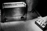
- FIG, 11. An auto radio operating solely from 11 developmental transistors. Eliminates the usual high-voltage power supply. Transistors operate from 6-volt storage battery. Receiver operates at 10% of usual battery drain

In the United States germanium is obtained most frequently as a by-product of zinc mining. It has also been obtained in considerable quantities in Great Britain from Hue dust residue. Manufacturers of germanium products receive this substance in the form of a germanium dioxide powder.
The conversion of the dioxide into crystals for use in transistors involves some of the most important and critical processes in the manufacture of germanium devices. The electrical characteristics of the transistor are dependent to a considerable degree upon the characteristics of the germanium. The control of transistor characteristics to acceptable tolerances depends upon the uniformity of the germanium.
.
The resistivity (die Sperrfähigkeit) of germanium
The resistivity of the germanium, an important factor in transistor operation, is dependent upon the presence in the germanium of minute quantities of certain impurities (künstliche Verunreinigung). If no impurities are present in the germanium crystal, no transistor action takes nlace. If too many impurity atoms are present, however, the germanium becomes too conductive and transistor action is adversely affected.
The impurities which enhance the transistor operation should be present in the ratio of less than one atom to every 10,000,000 germanium atoms.
Because of their exceedingly low concentration, it is quite difficult to detect the quantity of impurities present in the germanium crystal. Some of these impurities are actually present in the germanium dioxide as it is delivered to the manufacturer.
It is desirable, however, to remove as many impurities as possible by purification techniques (Säuberungstechniken) so that controlled amounts of them may be added to obtain the desired values of resistivity.
.
Die Umwandlung des Pulvers in Kristalle und Barren
The initial process in the conversion of germanium dioxide to the final crystals for transistor use is the reduction of the dioxide to a germanium metallic powder. This process is performed in a hydrogen atmosphere at a temperature of approximately 650 degrees Centigrade.
The powder is then melted at a temperature of approximately 960 degrees Centigrade and is formed into ingots (Blöcke oder Barren). After the ingots are formed, they may be subjected to one or more stages of purification. In one type of purification process, the germanium ingot is placed in a furnace of an inertgas atmosphere, is melted (geschmolzen), and then is progressively cooled from one end to the other.
During this cooling process, impurities present in the germanium tend to concentrate at each end of the ingot. The inner portion of the ingot, therefore, has a higher purity than the ends where the impurities are concentrated. The low-purity ends of the ingot may be cut off and the process repeated if additional purification is needed.
The germanium ingot formed by these purification techniques is polycrystallinc. Greater uniformity is obtained in a further process in which a single crystal is formed from this polycrystalline ingot. In this process the polycrystalline germanium is placed in a graphite pot and melted.
A small single crystal of germanium is dipped into the surface of the melt, then withdrawn very slowly, pulling with it some molten germanium which solidifies on the crystal seed. The speed of withdrawal may be about l/4 inch per minute. The temperature of the germanium is controlled very closely during the crystal "growing," with a permissible variation of no more than ±1 degree Centigrade.
.
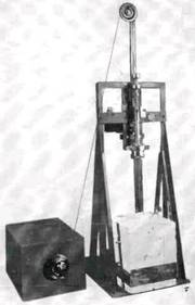
- FIG. 3. RCA's apparatus for "growing" the single germanium crystals used in making transistor units.

The crystal-growing apparatus and the price
Fig. 3 is a photograph of a crystal-growing apparatus. Single crystals ranging in diameter from 0.050 inch to one inch and having lengths up to many inches have been formed using this method.
Fig 12 is a photograph of the part of a single crystal which subsequently is to be "cut" into pellets (kleine Pillen oder Kügelchen) for assembly into transistors.
At the present time the price of the germanium dioxide powder is about 300.- dollars per kilogram. The quantity of germanium used for each transistor, however, is very small (about 0.002 gram).
The single crystal pictured in Fig. 12 can provide as many as 7.000 pellets for as many transistors, and many single crystals of this size can be obtained from one kilogram of germanium dioxide.
.
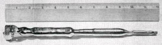
- FIG. 12. A single germanium crystal grown in the crystal-growing apparatus of Fig. 3.

Although a portion of the germanium is scrapped during the processing from powder to final crystal form, much of this germanium may be reclaimed for further use.
The finished crystal specimen is tested electrically to determine whether it has the proper impurity concentration, resistivity, and physical characteristics for use in transistors. The crystal is then sliced into wafers about 0.020 inch in thickness and diced into small pellets approximately 0.050 inch square. The pellets are chemically etched before the transistor is assembled to insure the absolute cleanliness of the crystal so necessary for good transistor operation.
.
Conductivity in Germanium (die Leitfähigkeit)
The germanium crystal is composed of millions of germanium atoms, each consisting of a positively charged nucleus and a number of negatively charged electrons. All but four of the electrons are tightly bound to the nucleus and cannot enter into chemical reactions with electrons of other atoms.
The remaining four electrons, which are able to enter into chemical processes, are called valence elections. In the pure germanium crystal, however, the atoms are arranged in such a fashion that the valence electrons are fixed in place and contribute only slightly to electrical conductivity. The resistivity, which is the reciprocal of conductivity, of the pure germanium, therefore, is higher than that of germanium containing impurities.
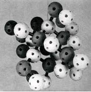
- FIG. 13. A three-dimensional model of the atomic structure of the germanium crystal.

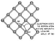
- FIG. 14. The effect of "p"-type impurities on the conductivity of germanium crystals.

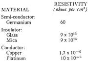
- TABLE 1. Resistivity of pure germanium. insulators, and conductors compared.

Die atomare Struktur
Fig. 13 is a photograph of a model of the atomic structure of a tiny portion of the germanium crystal. Each round ball represents the "nucleus" (Kern) of an atom, and each bar connecting two "nuclei" (Kerne) represents two valence electrons, one from each of the two atoms joined by the bar.
Each of the four valence electrons of an atom forms a bond with a valence electron from an adjacent atom. Electrons which are fixed in these electron-pair bonds cannot contribute to the conductivity of the crystal except under the influence of an applied force.
This condition is similar to that existing in an insulator, where there are no conduction electrons and, consequently, there is little or no conductivity. If sufficient electrical or thermal energy is exerted on the germanium crystals, however, the forces holding the electrons in their bonds can be overcome, and a few electrons may be released from their bonds.
Because of the release of electrons by thermal energy at room temperature, germanium does have some conductivity even in its pure state. The resistivity of pure germanium, a semiconductor, is 60 ohms per centimeter cube at room temperature.
The resistivity of insulators is much higher than that of semiconductors; that of metal conductors is much lower. In a metal conductor, there are a large number of conduction electrons which are not bound in a fixed position but are free to flow throughout the metal, thus contributing to a very low resistivity.
Table 1 gives a comparison of resistivities at room temperature of pure germanium, insulators, and conductors.
.
Die normale Leitfähigkeit
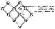
- FIG. 15. The effect of "n"-type impurities on the conductivity of germanium crystals.

The normal conductivity of germanium must be increased to obtain transistor operation. This additional conductivity is obtained by adding impurities to the crystal, as was mentioned previously.
The impurities which may be present in germanium are of three types. Fig. 15 illustrates how one type of impurity can add conduction electrons to the crystal. If impurities having five valence electrons per atom are added, each impurity atom (A) takes the place of a germanium atom and four of the five valence electrons form bonds with four electrons of adjacent germanium atoms.
The fifth electron (B) from the impurity atom is free to "wander" about the crystal and contributes to its conductivity in a manner similar to that of free electrons in a metallic conductor.
.
The npn type transistors
As more impurity atoms of this type are added, the conductivity of the germanium increases and the resistivity decreases. Germanium having an excess of electrons due to the addition of such impurities is known as "n"-type germanium, that is, germanium having an excess of negative charges.
"N"-type impurities are also known as "donor" impurities because they donate electrons to the crystal conductivity. Typical donor impurities are arsenic, antimony, and phosphorus.
The pnp type transistors
Conduction in germanium may also be increased by adding a second type of impurity such as aluminum, boron, or indium. Fig. 14 illustrates how these impurities, known as "p"-type impurities, create a deficiency of electrons. If impurities having three valence electrons per atom are added, each impurity atom (A) takes the place of a germanium atom and its three valence electrons form electron-pair bonds with electrons of neighboring germanium atoms.
In order to fit completely into the valence bond structure of the crystal, the impurity atom borrows an electron from an electron-pair bond from somewhere else in the crystal (B), thus leaving a net positive charge in the half-empty bond.
This positive charge is known as a "hole"; these holes contribute to the conductivity of the crystal in much the same manner as electrons because they also can move from atom to atom.
As more "p"-type impurities are added, more holes are formed and the conductivity of the crystal is increased. The main distinction between the two types of germanium is that the "n"-type has an excess of electrons while the "p"-type has an excess of holes.
Both "n" and "p" types are used in transistors: in certain types of transistors both exist in different parts of the same crystal. The "n"-type germanium is used predominantly in the present point-contact transistors.
.
Und eine "falsche" Verunreinigung des Germaniums geht gar nicht
The third type of impurity includes those which do not have three or five valence electrons. These impurities, which are present in very small quantities, may not affect the conductivity of the germanium, but may disturb the crystal structure and adversely affect transistor properties.
Die Dosierung ist extrem wichtig
The role which "p"-type and "n"-type impurities play in determining the resistivity of germanium may be appreciated by noting the change in resistivity which occurs with a change in the ratio of impurity atoms to germanium atoms.
The density of germanium atoms in pure germanium is approximately 4.5 x 10 hoch 22 atoms per cubic centimeter; there are approximately 3.7 x 10 hoch 19 germanium atoms in the average pellet used for a transistor. If 4.5 x l0 hoch 14 "n"-type impurity atoms are added to each cubic centimeter of pure germanium, or one impurity atom for every 100,000,000 germanium atoms, the resistivity of the germanium drops from 60 ohms per centimeter cube to approximately 3.8 ohm per centimeter cube, a value which is satisfactory for use in a point-contact transistor.
If 4.5 x 10 hoch 15 impurity atoms are added to the germanium, however, the resistivity drops to 0.38 ohms per centimeter cube, a value which is too low for transistor use.
This example illustrates how critical are the quantities of impurities which must be added. The problem is further complicated by the fact that "p"-type impurities may be present in the germanium ingot when the "n"-type impurities are introduced, and the holes and electrons furnished by the two types of impurities may cancel each other out.
If both type of impurities were present in equal amounts, the resistivity would be the same as if no impurities were present.
.
Fabrication Process
- Fig. 1


- Fig. 2

An appreciation of some of the unique characteristics of the transistor may be obtained from an examination of its construction. A photograph of an RCA developmental point-contact transistor is shown in Fig. 1.
Fig. 2 is a diagram of its construction. This transistor consists essentially of two rectifying point electrodes which make contact with a small pellet (Kügelchen) of germanium. These electrodes are known as the emitter and the collector.
A third electrode, the base, is in low-resistance contact with the germanium crystal.
The emitter, collector, and base form the three electrical connections to this germanium-crystal triode. The complete assembly is then embedded in a thermosetting plastic to provide rugged-ness and freedom from atmospheric contaminants.
The final process, and one of the most important, in transistor fabrication is electrical forming. In this process, relatively large surges of current are passed through the collector to the base.
.
Point-Contact Rectification
Before the operation of the transistor in specific circuits is covered, it is important to discuss briefly the current rectification obtained when the metal point electrode makes contact with the germanium-crystal surface.
When this contact occurs, a nonlinear relationship exists between a voltage applied to and the current flowing through the point of contact. A so-called "barrier" (eine Sperre) to the flow of current will be present or absent depending upon the polarity of the voltage applied to the metal point.
For instance, if a metal point contacts the surface of an "n"-type germanium, the barrier will be absent and a large forward current will flow if the metal point is biased positively with respect to the crystal.
If the point is biased negatively with respect to the crystal, the barrier will be present and only a small reverse current will flow. If the germanium is a "p"-type, the forward current will flow when the point is biased negatively with respect to the crystal.
One explanation of this barrier is that it is a very thin layer at the surface of the crystal which acts as an insulating layer. If the germanium resistivity is too low, this insulating barrier at the surface does not exist because of the large number of current carriers present both in the interior and on the surface of the germanium, and poor rectification results.
.
Der Verstärkungsfaktor (current amplification factor)
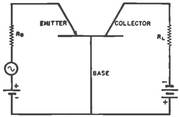
- FIG. 18. Transistor amplifier circuit.

Fig. 18 is a diagram of a transistor amplifier circuit utilizing the "n"-type transistor. In this circuit the collector is biased negatively with respect to the base. The emitter, also shown in Fig. 18, is biased positively with respect to the base.
If we first assume that no voltage is applied to the emitter, the collector will draw approximately 0.5 milliampere if a negative voltage of 25 volts is applied to the collector contact. Then, if a positive voltage is applied to the emitter contact, electrons will be drawn into the emitter and a flow of holes from the emitter will be attracted to the negative field of the collector, thereby increasing the collector current appreciably.
Now, with both the emitter and collector drawing current, a small signal voltage is applied to the transistor as indicated in the circuit diagram. As the applied voltage swings positive, the emitter current will increase, thereby increasing the collector current by supplying additional holes.
On the negative swing of the signal voltage, the collector current will decrease. If the assumption is made that every unit of hole current which leaves the emitter reaches the collector, it follows that a small change in emitter current will result in an equivalent change in collector current, producing a current amplification factor of one.
.
Die Definition des Verstärkungsfaktors
The current amplification factor is defined as the ratio of the change in collector current to a change in emitter current when the collector voltage is maintained constant.
A very significant characteristic of the transistor, however, is that this current amplification factor may actually be two or greater. Factors greater than unity are made possible by the electrical "forming" process.
One explanation of the results of this process is that a space charge of holes is formed around the collector point. It appears that this positive charge increases the electron flow from the metal collector to the germanium and account for the increased current amplification. *1)
*1) Shockley. W: "Electrons and Holes in Semiconductors." I). Van Nostrand, 1950.
The transistor amplifies not only input current, but also power. Because the emitter is biased in the forward direction, only a small impedance to the flow of current exists; therefore, the input impedance of the transistor is fairly low, on the order of 500 ohms. The collector, on the other hand, is biased in the reverse direction; it offers a higher impedance, therefore, to the flow of current.
The collector resistance comprises the greatest portion of the output impedance of the transistor. The load resistance, to provide a proper impedance match, must be fairly high, on the order of 10,000 to 20,000 ohms. With the input signal applied to the transistor at a low impedance and the output taken from a high impedance, power amplification results.
In the "p"-type transistor, electrons are emitted from a negatively biased emitter and are collected at a positively biased collector. In general, the "p"-type transistor has characteristics similar to the "n"-type unit, except that in operation all battery polarities are reversed.
.
Transistor Frequency Response
The frequency response of the point-contact transistor is limited by the "transit time" of the holes or electrons. Transit time is the time it takes the holes or electrons to travel from the emitter to the collector. The transit time in seconds may be calculated approximately through use of expressions.
Since an improved frequency response results from a small transit time, it can be seen from this expression that the response can be improved by using germanium of high resistivity and small contact spacings. The mobility of the holes or electrons is the velocity with which they move through the germanium when an electric field is applied.
In the case of "n"-type germanium, holes travel from the emitter to the collector; in the case of "p"-type germanium, electrons travel from the emitter to the collector. The mobility of electrons is greater than that of holes and, consequently, the frequency response of "p"-type germanium is slightly better than that of "n"-type germanium, provided that the contact spacings and resistivities are comparable.
The frequency response may be defined as the measure of the change in current amplification with increasing frequency. The current amplification factor of certain types of close-spaced point-contact transistors drops approximately 3db at 10 mc. A 3db drop in gain has been chosen to define the cut-off frequency.
This method of measuring frequency response, however, defines only one parameter as a function of frequency. If the power gain of the device is measured as a function of frequency in an amplifier with a high-impedance load, the response of the transistor deteriorates more rapidly. A transistor having a 3-decibel drop in the current amplification factor at 10 megacycles may have a cut-off of voltage or power gain at 4 megacycles or less.
.
Wide-Spaced Transistors
- FIG. 16. (Foreground) Transistors point way to new small-size units in electronic computers. Pencil points to one of five developmental point-contact transistors which do the job of the four tubes and four transformers of the rear unit.

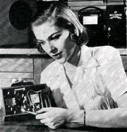
- FIG. 17. Transistors in an experimental personal.lype AM receiver developed at the David Sarnoll Research Center oi RCA at Princeton, N. I.. permit tremendous reduction in size, battery weight and power consumption.

The frequency of operation of point-contact transistors decreases fairly rapidly with increased point spacings. Since the transit time of the electrons or holes increases as the point spacing increases, in theory the frequency response of the transistor varies inversely as the cube of the spacing.
However, some interesting studies have been made of "n"-type transistors having wide spacings between contacts *1) and these devices appear to have some useful characteristics. If germanium having high resistivity is used, transistor power gain and current amplification are relatively independent of the separation of the points up to approximately 0.015 inch.
As the spacings increase, however, the effect of the collector upon the emitter decreases, that is, the feedback resistance decreases. A transistor having a feedback resistance of 200 ohms at 0.002-inch spacing of the contacts would have only 50 ohms at 0.015-inch spacing.
This value of feedback resistance for the wide-spaced transistors is low enough to assure short-circuit stability while values of power gain as high as 23 decibels are maintained. Even though the frequency-response limit varies inversely with the point spacing, the cutoff of the current amplification factor of the wide-spaced transistor is approximately 100 kilocycles because the resistivity of the germanium is higher than that used in narrow-spaced units. The other characteristics, except for the low internal feedback, are similar to those of the close-spaced transistor.
*1) Slade. B. T.: "A High Performance Transistor with Wide Spacing Between Contacts," RCA Review, Vol. XI. No. 4. page 517. December. 1950.
.
Power Considerations (Einschränkungen) I
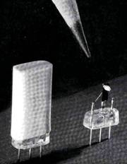
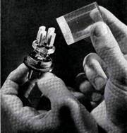
- FIG. 20. At right, pencil points to developmental junction-type transistor before embedment in plastic container. At left, the sealed unit.

The power capabilities
The power capabilities of point-contact transistors are low and considerably limit the use of these devices. Most point-contacl transistors do not withstand a collector power dissipation greater than 200 milliwatts.
If the efficiency of operation as a class A amplifier is assumed to be 30 percent, only 60 milliwatts of power output may be obtained from one stage of a transistor amplifier. A conservative figure for operation would be somewhere between 30 and 40 milliwatts.
There are, however, many applications in which some benefit may be obtained from a device which operates at low power dissipations. Consequently, the greatest opportunities for the use of point-contact transistors lie in those applications where power output is of relatively little importance and conservation of power is of primary importance.
Power Considerations (Einschränkungen) II
The power-handling capacity

- FIG. 7. A cigar-size experimental microphone-transmitter, modulated by a tiny built-in dynamic microphone. Employs two developmental junction type transistors, coil and battery.

The power-handling capacity of the point-contact transistor is limited largely because of thermal effects at the collector point. Considerable heat is generated at this point of contact when a current is passed through it.
Germanium is a fair conductor of heat and, consequently, some of the heat is conducted away from the point of contact through the germanium crystal and away from the crystal by the metal support.
If too large a value of current is passed, however, the germanium and adjacent parts are unable to carry the heat away rapidly enough. If the collector point becomes too hot, the collector resistance decreases and a change occurs in the collector bias current and also in the voltage drop across the collector.
Some permanent damage may occur if the transistor is operated at too high a dissipation. It is desirable, therefore, that the mechanical construction of the transistor be designed for the best possible heat conductivity away from the crystal.
By increasing the size of the crystal support and adding cooling fins, the allowable dissipation of the transistor may be increased to 500 milliwatts or more, thus increasing the power output of the transistor.
.
Höhere Leistung = geringere Verstärkung
The amount of conduction of heat away from the contact area varies inversely with the ambient temperature. As the ambient temperature is increased, the temperature at the point of contact becomes too great and the collector resistance is reduced. Changes in other properties of the transistor, such as the emitter resistance, transfer resistance, and internal feedback resistance, may also occur.
The net result of these changes is a loss of power gain, changes in bias conditions, and possible permanent damage to the transistor. For best operation, germanium transistors should be operated at temperatures below 60 degrees centigrade.
The maximum dissipation ratings of the device should also be reduced as ambient temperatures are increased above normal room temperature. At ambient temperatures below 25 degrees centigrade the situation is less critical, and if the temperature is low enough higher dissipations may be used without loss of stability.
* Wallace. R. L. Jr. and Pietenpol. W. J.: "Some Circuit Properties and Applications of N-P-N Transistors." Proceedings of the I.R.E. Vol. 39, No. 7. pages 753-767, July, 1951.
.
Junction Transistors
Other developmental germanium-crystal devices, known as "p-n" junction transistors, have somewhat different characteristics from those of the point-contact transistor. In comparison with currently produced point-contact types, the junction transistors have lower noise, higher power gain, greater efficiency of operation, and higher power-handling capabilities.
.

These improved characteristics, however, are not obtained without some loss in frequency response. Table 2 compares average values of several characteristics of the two types of transistors.
.
Es gibt 2 Typen von "junction transistors"
"point-contact transistor" versa "junction transistor"
- FIG. 19. Arrangement of "n" and "p" layers in an "n-p-n" type junction transistor.

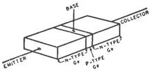
Two types of junction transistors have been developed. The "n-p-n" junction transistor *4) is composed of alternate n, p, and n layers of germanium - grown from a single crystal, as illustrated in Fig. 19.
The center layer of "p"-type germanium is very thin; its thickness may be as little as 0.001 inch. Low-resistance contacts to the "n"-areas form the emitter and collector, and a low-resistance connection to the "p"-layer constitutes the base terminal.
The principle of operation of the "junction transistor" is somewhat different from that of the "point-contact transistor" in that the rectification takes place at the junctions between the p- and n-type layers rather than at point contacts.
In the point-contact transistor, holes or electrons drift from the emitter to the collector under the influence of electric fields. In the "n-p-n" junction transistor, electrons diffuse through the p-type layer and are attracted to the collector.
The center layer has an excess of holes, but if this layer is thin enough, most of the electrons entering the base region from the "mutter" (Gemurmel, Gemisch) will reach the collector region without recombining with the holes. Practically all the electrons leaving the emitter reach the collector, thus resulting in a current amplification of approximately one, but this type of transistor cannot attain current amplifications greater than one unless more complex junctions are introduced.
High power gains are obtained as a result of the tremendous impedance step-up between input and output circuits. The emitter junction is biased in the forward direction, and since the forward resistance of the junction is very low, the input impedance of the device is as low as 25 to 100 ohms.
The resistance of the collector junction, which is biased in the reverse direction, is very high, on the order of several megohms, thus resulting in a very high output impedance. This tremendous difference in impedances can result in power gains of over 40 decibels.
.
The "p-n-p" junction transistor
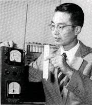
- FIG. 24. Dr. C. W. Mueller of the research staff of the David Sarnoff Research Center of RCA Princeton. N. J., points to a "blown-up" model of the heart of an RCA developmental junction-type transistor. Complete interior model is seen at right. A "p-n-p" junction-type transistor is shown in the inset at lower right

Another junction device, the "p-n-p" transistor (see inset Fig. 24), is formed by diffusing two "p"-type impurity metals on opposite faces of a piece of "n"-type germanium.
Atoms diffuse from these impurity metals into the germanium at high temperatures converting a portion of the "n"-type germanium to "p"-type, thus forming "p-n" junctions.
In this transistor, the emitter is biased positively with respect to the base, and the collector is biased negatively with respect to the base. Hole carriers are injected by the emitter and arrive at the collector, resulting in a current amplification factor of approximately one, as in the "n-p-n" transistor.
An appreciation of some of the most outstanding qualities of the junction transistor may be obtained from a study of the output characteristics. The junction transistor has a constant current amplification factor and output resistance down to very low collector voltages.
Operation with power inputs as low as 0.6 microwatt have been reported. This input is about one-ten-thousandth the power dissipation required to operate the point-contact transistor, and less than one-millionth the power required to heat the cathode of most vacuum tubes. The almost ideal static characteristics show that the junction transistor can operate close to 50% efficiency as a class A amplifier. Although the junction transistors for which these characteristics are plotted can operate at only limited power dissipations, approximately 50 milliwatts, design of these devices for operation at 2 watts or greater is possible.
.
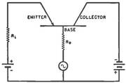
Vergleiche mit Verstärkerschaltungen
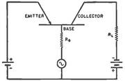
- FIG. 21. Layout whereby the transistor is used in grounded-base amplifier circuit.

- FIG. 22. A transistor grounded-emitter amplifier circuit, as discussed in the text.

- FIG. 23. The transistor grounded'Coliector amplifier circuit. See the text for details.

It is interesting to compare the amplifier circuit properties of the point-contact transistor and the junction transistor.
A number of amplifier circuit connections are possible to obtain several combinations of input and output impedances. In the case of the point-contact transistor, however, special consideration must be given to the circuitry. If the internal feedback resistance is too large, and if the current amplification factor is greater than unity, the circuit may become unstable and oscillations will occur.
The internal feedback resistance varies with the operating point. The current amplification factor may also vary somewhat with collector voltage, thus making the circuit stability dependent upon the d.c. biases.
Resistance placed in series with the emitter and collector leads helps to suppress these oscillations, but may decrease the power gain of the circuit. For example, the input impedance to the grounded-base amplifier circuit shown in Fig. 21 is approximately 500 ohms and the output impedance is approximately 10.000 ohms.
If the internal feedback "resistance" (?) is too large, additional resistance necessary to stabilize the circuit will exceed these impedance values and, therefore, reduce the gain of the circuit. Point-contact transistors which have a very low value of internal feedback resistance, less than 100 ohms, for example, usually have such low feedback that amplifier circuits require no special stabilization.
It is desirable in some r.f. circuits, particularly, that the transistor be stable under low impedance conditions such as off-resonance of a parallel-tuned circuit.
In the case of the simple junction transistor, the current amplification factor is always less than unity, and oscillations cannot occur.
Ryder and Kircher" have pointed out that the grounded-base circuit is analogous to an electron-tube grounded-grid circuit if the emitter, base, and collector of the transistor are compared to the cathode, grid, and plate of the electron tube, respectively.
The grounded-grid electron-tube circuit also has a low input and high output impedance. The comparison is particuarly appropriate in the case of the junction transistor, which, like the tube circuit, is stable even under extreme short-circuit conditions.
If the emitter is grounded, as in Fig. 22, higher input impedances and lower output impedances may be obtained. Higher power gains may be obtained with this circuit configuration than with the grounded-base circuit, but in point-contact transistors the feedback may become large and lead to instability. If junction transistors are used, this type of circuit is similar to an electron-tube grounded-cathode circuit.
Higher input impedances and lower output impedances may also be obtained if the collector is grounded, as in Fig. 23. This circuit can become unstable if a point-contact transistor is used, and the power gain which may be obtained is low.
However, the junction transistor can be used to good advantage in this circuit, because power gains ranging from 10 to 20 db may be obtained with input impedances and output impedances on the order of 200,000 and 50,000 ohms, respectively.
In fact, appreciable gain may be obtained using equal input and output matching impedance, thus making cascading of several stages of amplification feasible. This circuit is similar to the electron-tube grounded-plate or conventional cathode-follower circuit.
*6) Ryder, R. M. and Kirelier. R. J.: "Sonic Circuit Aspects <if the Transistor." Bell System Technical Journal. Vol. XXVIII, pages 367-401. July 1949.
.
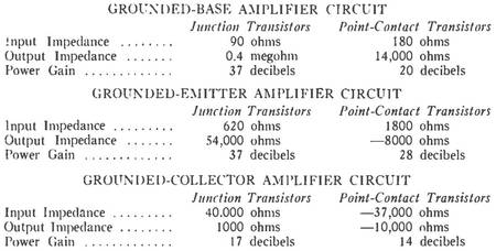
- TABLE 3. Typical values of input and output impedances and power gains for all three types of circuits for both junction-type and point-contact transistors.

Table 3 shows typical values of input and output impedances and power gains for all three types of circuits for both junction-type and point-contact transistors. It will be noted that in the grounded-emitter and grounded-base circuits the input and output impedances of the point-contact transistor may actually become negative values, a condition which indicates that these circuits are potentially unstable. These characteristics of the point-contact types, which lead to potential instability in amplifiers, are of great advantage in oscillators and trigger devices.
.
Other Circuit Applications
When considering the possible circuit applications for the two types of transistors, one must be aware of the advantages and limitations of both types.
At the present time, the advantages of high gain, low noise, and greater stability of the simple junction transistor can be utilized at frequencies up to several megacycles in applications such as r.f. and i.f. amplifiers of standard broadcasting receivers.
In addition, power outputs greater than one watt appear to be possible in oscillator and amplifier applications in the audio frequency and low frequency ranges. Another feature of the junction transistor is its ability to amplify and oscillate with microwatt power inputs.
The frequency response of the point-contact transistors, on the other hand, is somewhat higher than that of junction types. As with junction types, point-contact types which are currently available, can be made to oscillate and amplify over the broadcast-frequency band. When used as an amplifier, point-contact transistors have a relatively flat response over the entire broadcast band and beyond.
Types now under development will operate at considerably higher frequencies. Feedback in these units has been reduced to values which make stable operation at radio frequencies practical. The point-contact transistor therefore, may also have considerable application in radio circuits and may be used in intermediate-frequency amplifiers, radio-frequency oscillators, and other circuits not associated with the high-power stages of r.f. systems.
Point-contact transistors have been developed which are capable of oscillating at frequencies well over 100 mc. Oscillations at frequencies higher than 200 mc. have been obtained - one developmental unit has oscillated at a frequency over 300 mc.
.
Transistoren in "counter circuits"
One of the most important uses of the point-contact transistor probably will be in counter circuits. A number of recent publications describe some basic circuits which utilize the negative resistance properties of one or more transistors.
These circuits generate pulses of various waveforms, store information for varying periods of time, add, subtract, multiply, and divide. Up to the present time these functions, and many others, have been performed in electronic computers by large numbers of electron tubes for which the heater-power supplies alone have been considerable.
Use of the transistor would obviously alleviate this situation since no heater power is required. Furthermore little d.c. power is necessary for operation. The adverse characteristics of transistors with regard to frequency response, noise and power output are relatively unimportant factors in computer circuits. Computers which employ germanium devices would have the advantages of small size, ruggedness, and economy of operation and maintenance.
Other Germanium Devices
The progress in the field of germanium devices is not limited to the field of transsistors. While the point-contact germanium diode has already attained commercial acceptance, new types of diodes utilizing the "p-n" junction rectification characteristics are being developed. One diode power rectifier which utilizes a p-type or acceptor impurity metal diffused onto a pellet of germanium has already been described. *8)
Peak inverse voltages of 400 volts are permissible with these devices which have very low resistances in the forward direction and current-carying capabilities as high as 350 milliamperes. When the relative infancy of the germanium power rectifier is considered, it is difficult to estimate the ultimate importance of these devices.
Because of improved efficiency, however, they appear to be suitable both as a replacement for the selenium rectifier and as an advantageous substitute for certain types of rectifier tubes.
.
*7) Eberhard. E.. Endrey, R. O.. and Moore.
R. P.: "Counter Circuits Using Transistors."
RCA Review, Vol. X, No. 4, page 459. December 1949.
*8) Saby. J. S.: "Recent Developments in Transistors and Related Devices" Tele-Tech, Vol, 10, No. 12. December, 1951.
The phototransistor
Another germanium device of considerable significance is the phototransistor. *9) This photocell is a photo-conductive device and operates on the principle that light absorbed by germanium changes its conductivity. In the phototransistor, a point contact acts as the collector and draws a small amount of current. Light in the vicinity of the collector increases the conductivity of the germanium and the current through the collector.
The first transistor was announced only three and one-half years ago. Great strides have been made in learning the fundamental theory of operation of transistor devices, and much progress has been made in the knowledge of the control of transistor characteristics and manufactuting processes.
There appear to be a number of fields in which transistors will be used widely and to great advantage. Further improvements in their characteristics may be expected as research and development continue.
Acknowledgment
The author wishes to acknowledge the advice and contributions of Mr. E. W. Herold and Dr. J. Kurshan of the RCA Laboratories Division, Princeton, N. J. and of Mr. R. M. Cohen and Mr. H. Nelson of the RCA Tube Department. Harrison, N. J.